- 您现在的位置:买卖IC网 > Sheet目录319 > CPC5002G (IXYS Integrated Circuits Division)ISOLAT DGTL 3.75KVRMS 2CH 8-DIP
�� �
�
�I� NTEGRATED� C� IRCUITS� D� IVISION�
�3.3� Output� Drivers�
�Designed� specifically� for� data� and� clock� busses,� the�
�output� drivers� have� been� configured� for� optimal�
�performance� and� behavior.�
�To� reduce� RF� emissions� and� ringing� on� the� output�
�lines� the� active� low� output� drivers� are� slew� limited.� In�
�addition� to� limiting� emissions,� the� slew� limited� outputs�
�reduce� the� need� for� external� output� series� resistors.�
�Whenever� the� outputs� are� in� the� deasserted� logic� high�
�state,� the� open-drain� outputs� exhibit� low� leakage�
�performance� while� presenting� a� high� impedance�
�(Hi-Z)� to� the� load.� Additionally,� during� power-up� and�
�CPC5002�
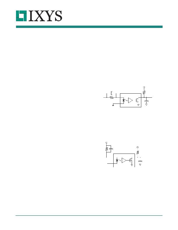
�4� Circuit� Examples�
�4.1� Inverting� and� Non-Inverting� Configurations�
�Shown� below� are� typical� inverting� and� non-inverting�
�circuit� examples� with� the� optional� feed� forward�
�capacitors� used� for� high� speed� signals.�
�These� designs� assume� a� combined� voltage� drop� of�
�3.3V� across� the� input� resistor� and� the� LED� with� a�
�nominal� input� current� of� 1.5mA.�
�Figure� 1.� Inverting� Configuration�
�with� the� loss� of� V� DD� ,� the� outputs� default� to� the� Hi-Z�
�deasserted� state� thereby� ensuring� signal� integrity� of�
�any� bussed,� open-drain� signals� connected� to� the�
�output� pins�
�V� I� N�
�C� F� W� D�
�10pF�
�1/2� CPC5002�
�3.3� V�
�R� PU�
�499� Ω�
�V� OUT�
�To� maximize� system� design� flexibility,� the� outputs� are�
�tolerant� of� pull-up� voltages� greater� than� the� CPC5002�
�supply� voltage,� V� DD� ,� provided� the� pull-up� voltage�
�remains� within� the� output’s� specified� voltage� limits.� For�
�example,� using� a� 3.3V� supply� to� power� the� CPC5002,�
�it’s� outputs� may� be� safely� operated� into� a� pull� up�
�1.4k�
�In� v� erting:� V� I� N� to� V� OUT�
�C� L�
�20pF�
�resistor� to� a� supply� voltage� of� 6.5V.�
�C� FWD� increases� instantaneous� I� F� at� LED� turn-on� to�
�reduce� t� PHL� at� V� OUT� .�
�3.4� Power� Supply� Decoupling� and� Noise�
�Reduction�
�There� are� no� special� power� supply� decoupling�
�Figure� 2.� Non-Inverting� Configuration�
�V� +�
�requirements� for� the� CPC5002.�
�In� addition,� since� the� CPC5002� uses� optical� coupling�
�to� transfer� information� across� the� barrier,� no� internal�
�clocking� circuits� are� utilized� to� maintain� the� proper�
�output� state.� This� negates� the� need� to� implement� the�
�1.4k�
�V� I� N�
�C� F� W� D�
�10pF�
�1/2� CPC5002�
�3.3� V�
�R� PU�
�499� Ω�
�V� OUT�
�C� L�
�20pF�
�required� special� layout� or� noise� reduction� techniques�
�necessary� to� maintain� EMI� or� RFI� compliance.�
�N� on-In� v� erting:� V� I� N� to� V� OUT�
�For� applications� where� the� nominal� total� voltage� drop�
�across� the� input� resistor� and� the� LED� is� not� 3.3V� it� will�
�be� necessary� to� adjust� the� input� resistor’s� value.�
�Examples� of� this� would� be� different� pull-up� voltage�
�supplies� and� V� IN� sources� that� do� not� drive� completely�
�to� the� supply� rails.�
�R03�
�www.ixysic.com�
�9�
�发布紧急采购,3分钟左右您将得到回复。
相关PDF资料
CPCI-D-3U-300C
PWR SUPLY DC/DC CPCI 300W 3UX8HP
CPD250-4530G
PWR SUP 250W 3.3/5/12/-12V QUAD
CS4161YN8
IC DRIVER H-BRDG DUAL 85MA 8DIP
CS5461A-ISZ
IC ENERGY METERING 1PHASE 24SSOP
CS5462-ISZ
IC ENERGY METERING 1PHASE 24SSOP
CS5463-IS
IC PWR/ENERGY METER 2CH 24-SSOP
CS5464-IS
IC PWR/ENERGY METER 3CH 28-SSOP
CS5466-ISZR
IC ENERGY METERING 1PHASE 24SSOP
相关代理商/技术参数
CPC5002GS
制造商:IXYS Integrated Circuits Division 功能描述:Digital Isolator Open Drain 2-CH 10Mbps 8-Pin PDIP SMD Tube
CPC5002GSTR
功能描述:ISOLAT DGTL 3.75KVRMS 2CH 8-SMT RoHS:是 类别:隔离器 >> 数字隔离器 系列:- 标准包装:66 系列:iCoupler® 输入 - 1 侧/2 侧:2/2 通道数:4 电源电压:3.3V,5V 电压 - 隔离:2500Vrms 数据速率:25Mbps 传输延迟:60ns 输出类型:逻辑 封装/外壳:20-SSOP(0.209",5.30mm 宽) 供应商设备封装:20-SSOP 包装:管件 工作温度:-40°C ~ 105°C
CPC51
制造商:CROMPTON LIGHTING 功能描述:DIFFUSER PRISMATIC SINGLE 5FT
CPC510J
制造商:Mallory Sonalert Products Inc 功能描述:Cap Ceramic 51pF 1000V C0G 5% (9.5 X 4.5mm) Radial 6.4mm 125°C 制造商:CORNELL DUBILIER ELECTRONICS 功能描述:Cap Ceramic 51pF 1000V C0G 5% (9.5 X 4.5mm) Radial 6.4mm 125°C
CPC52
制造商:CROMPTON LIGHTING 功能描述:DIFFUSER PRISMATIC TWIN 5FT
CPC5601
制造商:CLARE 制造商全称:Clare, Inc. 功能描述:Auxiliary Programmable Driver IC
CPC5601D
功能描述:固态继电器-PCB安装 Programmable Driver IC RoHS:否 制造商:Omron Electronics 控制电压范围: 负载电压额定值:40 V 负载电流额定值:120 mA 触点形式:1 Form A (SPST-NO) 输出设备:MOSFET 封装 / 箱体:USOP-4 安装风格:SMD/SMT
CPC5601DTR
功能描述:固态继电器-PCB安装 Programmable Driver IC, T/R RoHS:否 制造商:Omron Electronics 控制电压范围: 负载电压额定值:40 V 负载电流额定值:120 mA 触点形式:1 Form A (SPST-NO) 输出设备:MOSFET 封装 / 箱体:USOP-4 安装风格:SMD/SMT